Electron Microscope and Energy Dispersive Spectroscopy

Understand Electron Microscope and Energy Dispersive Spectroscopy. Learn about their applications in material science and advancements in technology.
The Basics of Electron Microscope
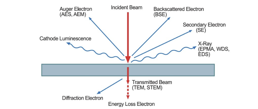
An electron microscope is a powerful scientific instrument that uses a beam of accelerated electrons to magnify objects up to millions of times their actual size. Unlike traditional light microscopes, which use light waves to create magnified images, electron microscopes use a beam of electrons that interact with the specimen to create detailed images with much higher resolution.
There are two main types of electron microscopes: transmission electron microscopes (TEM) and scanning electron microscopes (SEM). TEMs are used to examine thin slices of specimens and provide high-resolution images of internal structures. SEMs, on the other hand, are used to study the surface of specimens and provide detailed three-dimensional images.
Electron microscopes have revolutionized scientific research by allowing scientists to study the intricate details of objects at the nanoscale. They have been instrumental in various fields such as biology, materials science, and nanotechnology.
Understanding Energy Dispersive Spectroscopy
Energy Dispersive Spectroscopy (EDS) is a technique used in conjunction with electron microscopy to analyze the elemental composition of a sample. It involves the detection and quantification of characteristic X-rays emitted from the sample when it is bombarded with high-energy electrons.
By measuring the energy and intensity of these X-rays, scientists can identify the elements present in the sample and determine their relative abundance. EDS is particularly useful for studying the chemical composition of materials, identifying impurities or contaminants, and mapping the distribution of elements within a sample.
EDS has found applications in various scientific disciplines, including materials science, geology, forensic science, and environmental analysis. It provides valuable insights into the composition and structure of materials, aiding in the development of new materials and the understanding of natural processes.
Applications in Material Science
Electron microscope and Energy Dispersive Spectroscopy have numerous applications in the field of material science. They enable scientists to study the microstructure and composition of materials at the atomic and nanoscale, providing valuable insights into their properties and behavior.
One application of electron microscopy and EDS is in the characterization of materials for various industries, such as semiconductor manufacturing, aerospace, and automotive. By analyzing the microstructure and elemental composition of materials, scientists can assess their quality, identify defects or impurities, and optimize their performance.
Another application is in the field of nanotechnology, where electron microscopy and EDS are used to visualize and analyze nanomaterials. These techniques help scientists understand the unique properties of nanomaterials and develop innovative materials with enhanced performance.
Furthermore, electron microscopy and EDS are also used in materials research and development. Scientists can study the structure-property relationships of materials, investigate phase transformations, and explore new materials with specific functionalities.
Overall, the applications of electron microscopy and EDS in material science are vast and contribute significantly to advancements in various industries and scientific fields.
Advancements in Technology
Over the years, there have been significant advancements in electron microscope and Energy Dispersive Spectroscopy technology, leading to improved performance and capabilities.
One major advancement is the integration of electron microscopy with other techniques, such as spectroscopy and microscopy. This enables simultaneous imaging and chemical analysis of samples, providing a more comprehensive understanding of their properties.
Furthermore, there have been improvements in detector technology for EDS, resulting in higher sensitivity and faster data acquisition. This allows for more efficient elemental analysis and mapping of samples.
Additionally, advancements in software and data processing algorithms have made it easier to analyze and interpret the large amounts of data generated by electron microscopy and EDS. This has facilitated more efficient and accurate characterization of materials.
These technological advancements continue to push the boundaries of electron microscopy and EDS, opening up new possibilities for scientific research and discoveries.


