Understanding the Plasma Etching Process in Semiconductor Technology

Explore the world of etching in semiconductor technology and discover its crucial role in manufacturing semiconductor devices.
The Basics of Etching
Etching is a crucial process in semiconductor technology that involves selectively removing material from the surface of a semiconductor wafer.
The main purpose of etching is to create patterns or structures on the wafer surface that are essential for the functioning of semiconductor devices.
There are two main types of etching: wet etching and dry etching.
Wet etching involves using liquid chemicals to remove the material, while dry etching uses plasma or reactive gases.
Etching can be done using various techniques such as chemical etching, physical etching, and plasma etching.
Types of Etching
Wet etching: This type of etching involves immersing the semiconductor wafer in a liquid etchant solution.
The etchant reacts with the exposed parts of the wafer surface and removes the material selectively.
Dry etching: This type of etching does not use a liquid etchant solution.
Instead, it relies on plasma or reactive gases to remove the material from the wafer surface.
Dry etching is further classified into two types: physical etching and chemical etching.
Physical etching involves physical bombardment of the wafer surface with ions or neutral particles to remove the material.
Chemical etching, on the other hand, involves using reactive gases to chemically react with the material and remove it from the wafer surface.
The Basics of Plasma Etching
Plasma etching is a type of dry etching technique that uses plasma to remove material from the semiconductor wafer surface.
Plasma is a highly ionized gas that contains a mixture of ions, electrons, and neutral particles.
Plasma etching is widely used in semiconductor manufacturing due to its high precision and control over the etching process.
The plasma etching process involves the following steps:
- Generation of plasma: A plasma source is used to create a plasma environment.
- Activation of the etchant gas: The etchant gas is introduced into the plasma, where it gets ionized and reactive.
- Selective etching: The reactive ions and radicals in the plasma selectively react with the material on the wafer surface and remove it.
Plasma etching can be used for various applications such as etching patterns, creating trenches, and removing unwanted material.
Types of Plasma Etching
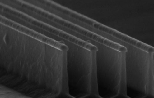
There are two main types of plasma etching: isotropic etching and anisotropic etching.
Isotropic etching: This type of etching removes material in all directions, resulting in rounded or tapered features.
Anisotropic etching: This type of etching removes material preferentially in a specific direction, resulting in vertical or near-vertical sidewalls.
Advantages and Disadvantages of Plasma Etching
Plasma etching offers several advantages over other etching techniques in semiconductor manufacturing:
- High selectivity: Plasma etching allows for highly selective removal of material, resulting in precise patterns and structures.
- High etch rate: Plasma etching can achieve a high etch rate, allowing for faster manufacturing processes.
- Good uniformity: Plasma etching provides good uniformity across the wafer surface, ensuring consistent results.
However, there are also some disadvantages associated with plasma etching:
- Complexity: Plasma etching is a complex process that requires specialized equipment and expertise.
- Cost: The equipment required for plasma etching can be expensive, making it less accessible for small-scale manufacturing.
- Damage to sensitive materials: Plasma etching can cause damage to sensitive materials or structures on the wafer surface.
Despite these disadvantages, plasma etching remains a crucial process in semiconductor technology due to its unique advantages.