Advancing Precision: The Power of Focused Ion Beam Technology

Explore how Focused Ion Beam (FIB) technology revolutionizes materials science and precision manufacturing.
Revolutionizing Microscale Machining: Precision and Control
Focused Ion Beam (FIB) technology has revolutionized microscale machining by providing exceptional precision and control. With FIB, researchers and manufacturers can achieve high-resolution machining. This level of precision allows for the creation of intricate structures and patterns on a microscale, enabling advancements in various industries such as electronics, optics, and nanotechnology.
Furthermore, FIB offers unparalleled control over the machining process. The ion beam can be precisely directed to remove material at specific locations, allowing for the creation of complex shapes and features. This level of control is crucial in applications where precision is paramount, such as the fabrication of microelectromechanical systems (MEMS) and integrated circuits.
Overall, FIB technology has transformed microscale machining by providing unprecedented precision and control, enabling the creation of intricate structures and advancing various industries.
Enhancing Material Analysis with Focused Ion Beams
Focused Ion Beam (FIB) technology has greatly enhanced material analysis capabilities. By using a focused ion beam to remove material from a sample, researchers can access and analyze the internal structure of the material at a high resolution.
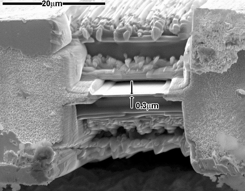
FIB allows for cross-sectional analysis, where a thin slice of the material is cut using the ion beam. This cross-sectional view provides valuable insights into the material's composition, layer structure, and defect distribution. It is particularly useful in semiconductor analysis, allowing researchers to study the quality of thin films, interfaces, and device structures.
Moreover, FIB technology enables site-specific analysis, where specific regions of interest can be targeted for further investigation. This capability is essential in failure analysis, where identifying the root cause of a defect or failure is crucial for improving product reliability.
In summary, FIB technology enhances material analysis by providing high-resolution cross-sectional views and enabling site-specific analysis, empowering researchers to gain valuable insights into material properties and improve product performance.
Applications in Semiconductor Manufacturing
Focused Ion Beam (FIB) technology plays a vital role in semiconductor manufacturing. It offers several advantages that make it indispensable in this industry.
One of the key applications of FIB in semiconductor manufacturing is circuit edit and repair. FIB allows for precise modification and repair of integrated circuits by selectively adding or removing material. This capability is crucial in the development and debugging of semiconductor devices, enabling quick modifications and improvements without the need for complete redesigns.
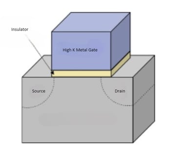
Another important application is the fabrication of nanoscale devices. FIB can be used to create nanostructures, such as nanowires and nanodots, with high precision. These structures are essential for the development of advanced semiconductor devices, nanoscale transistors, and sensors.
Furthermore, FIB technology is utilized in the analysis and characterization of semiconductor devices. It enables the extraction of small samples for transmission electron microscopy (TEM) analysis, allowing researchers to study the internal structure and defects at the atomic level.
Overall, FIB technology has become an integral part of semiconductor manufacturing, enabling circuit edit and repair, nanoscale device fabrication, and advanced analysis of semiconductor devices.
Improving the Efficiency of Failure Analysis
Focused Ion Beam (FIB) technology has greatly improved the efficiency of failure analysis in various industries.
Failure analysis is a crucial process in investigating the causes of defects or failures in materials and products. FIB technology offers unique capabilities that expedite this process and provide valuable insights into the root causes of failures.
One of the key advantages of FIB in failure analysis is the ability to perform site-specific sample preparation. The focused ion beam can precisely mill away material from a specific region of interest, exposing the underlying layers and defects.
Moreover, FIB enables in situ analysis during the sample preparation process. Researchers can use imaging techniques, such as scanning electron microscopy (SEM) and focused ion beam microscopy (FIB-SEM), to monitor the milling progress and identify potential defects or anomalies in real-time. This real-time feedback enhances the efficiency and accuracy of failure analysis, enabling faster identification of root causes and more effective corrective actions.
In summary, FIB technology improves the efficiency of failure analysis by enabling site-specific sample preparation and in situ analysis, ultimately leading to faster identification of root causes and more efficient problem-solving.
Focused Ion Beam Milling
Focused Ion Beam (FIB) milling is a versatile technique that offers several advantages in materials processing.
One of the key advantages of FIB milling is the high precision and resolution it provides. The focused ion beam can be precisely controlled to remove material with sub-nanometer accuracy, allowing for the fabrication of complex structures and features on a microscale. This level of precision is crucial in applications where tight tolerances and intricate geometries are required.
Furthermore, FIB milling can be performed on a wide range of materials, including metals, semiconductors, ceramics, and polymers. This versatility makes it suitable for various industries, from electronics and optics to biotechnology and aerospace.
Another advantage of FIB milling is the ability to perform three-dimensional (3D) machining. By controlling the ion beam's direction and intensity, complex 3D structures can be created with high precision. This capability is particularly valuable in the fabrication of microelectromechanical systems (MEMS), where intricate 3D structures are essential for device functionality.
In summary, FIB milling offers high precision, versatility, and the ability to create complex 3D structures, making it a powerful technique in materials processing.
Advanced Techniques in Ion Beam Etching and Deposition
Focused Ion Beam (FIB) technology has advanced techniques in ion beam etching and deposition, enabling precise material modification and fabrication.
Ion beam etching is a process where material is selectively removed by bombarding it with energetic ions. FIB allows for precise control over the ion beam, enabling the etching of complex patterns and structures with high accuracy. This capability is essential in the fabrication of nanoscale devices and integrated circuits, where precise patterning is required.
On the other hand, ion beam deposition involves the controlled deposition of material onto a substrate using the ion beam. FIB enables the deposition of a wide range of materials, including metals, insulators, and semiconductors. This capability is valuable in the fabrication of thin films, coatings, and nanostructures.
Moreover, FIB technology enables the combination of etching and deposition in a single system, known as focused ion beam-induced deposition (FIBID). This technique allows for the precise fabrication of complex 3D structures by selectively depositing material in desired locations while simultaneously etching unwanted material.
In summary, FIB technology has advanced ion beam etching and deposition techniques, enabling precise material modification and fabrication of complex structures.
Imaging with Focused Ion Beams
Focused Ion Beam (FIB) technology offers powerful imaging capabilities that allow researchers to visualize and analyze samples at a high resolution.
FIB can be used for imaging through two main techniques: secondary electron imaging and ion beam-induced secondary electron imaging.
Secondary electron imaging involves detecting the secondary electrons emitted from the sample surface when it is bombarded by the ion beam. This technique provides high-resolution images with excellent topographical contrast, allowing researchers to observe surface features and textures in detail.
Ion beam-induced secondary electron imaging, on the other hand, involves detecting the secondary electrons emitted by the ion beam itself as it interacts with the sample. This technique offers excellent material contrast and enables the visualization of subsurface structures and interfaces.
Both imaging techniques can be combined with other analytical techniques, such as energy dispersive spectroscopy (EDS) and electron backscatter diffraction (EBSD), to obtain comprehensive information about the sample's composition, crystal structure, and elemental distribution.
In summary, FIB technology provides powerful imaging capabilities through secondary electron imaging and ion beam-induced secondary electron imaging, enabling researchers to visualize and analyze samples at a high resolution.


