Revolutionizing Semiconductor Manufacturing: The Impact of Microscopic Images and Deep Learning
In this blog post, we will dive into the incredible impact of microscopic images and cutting-edge microscopic image analysis technologies on the world of semiconductor manufacturing. Discover how these advancements are revolutionizing the industry and driving innovation to new heights.
The Evolution of Semiconductor Manufacturing
Semiconductor manufacturing has come a long way since its inception. From the early days of manual production to the high-tech processes of today, the industry has witnessed a remarkable evolution. With advancements in technology and increasing demand for smaller, faster, and more efficient devices, semiconductor manufacturers have had to continuously adapt and innovate.
In the early years, semiconductor manufacturing involved painstakingly placing individual components on a wafer, a process known as discrete component assembly. This method was time-consuming and prone to errors. However, as the industry grew, manufacturers began to explore new techniques such as integrated circuit (IC) fabrication. This involved using photolithography to etch patterns onto a silicon wafer and then depositing various layers of materials to create transistors and other electronic components.
Over time, semiconductor manufacturing techniques continued to improve. The introduction of cleanrooms, where the air is filtered to remove contaminants, helped to ensure the quality of the final product. Automation also played a significant role in streamlining the production process, allowing for higher precision and efficiency.
The Role of Microscopes in Semiconductor Manufacturing
Microscopes play a crucial role in semiconductor manufacturing. They are used for various purposes, including inspection, quality control, and failure analysis. By providing magnified views of semiconductor materials and components, microscopes enable manufacturers to identify defects, measure dimensions, and ensure the overall quality of the final products.
One of the most commonly used microscopes in semiconductor manufacturing is the scanning electron microscope (SEM). SEMs use a focused beam of electrons to scan the surface of a sample, generating high-resolution images. These images provide valuable information about the structure, composition, and morphology of semiconductor materials.
In the context of semiconductor manufacturing, SEM images are particularly useful for analyzing and characterizing the features of semiconductor devices. They can reveal details such as the size and shape of gates, the presence of defects or contaminants, and the overall uniformity of the materials. SEM images can also help in identifying process issues and optimizing manufacturing parameters.
Overall, microscopes, especially SEMs, are indispensable tools in semiconductor manufacturing. They enable manufacturers to ensure the quality and reliability of their products, improve process efficiency, and drive innovation in the field.
Exploring Use Cases of Scanning Electron Microscope Images
Scanning electron microscope (SEM) images have various use cases in semiconductor manufacturing. Here are some examples:
1. Defect Analysis: SEM images can be used to identify and analyze defects in semiconductor materials and devices. By closely examining the images, manufacturers can pinpoint issues such as broken bonds, contamination, or irregularities in the crystal structure.
2. Dimensional Measurements: SEM images allow for precise measurements of semiconductor features, such as line widths, contact sizes, and transistor dimensions. These measurements are essential for ensuring that the devices meet the required specifications and performance standards.
3. Process Optimization: SEM images can provide valuable insights into the effectiveness of manufacturing processes. By analyzing the images, manufacturers can identify process variations, evaluate the impact of process parameters, and optimize the fabrication techniques to achieve better yields and quality.
4. Failure Analysis: When semiconductor devices fail, SEM images can be used to investigate the root causes. By examining the images of the failed components, manufacturers can determine whether the failure was due to material defects, manufacturing issues, or external factors such as electrical overstress or thermal stress.
These are just a few examples of the many use cases of SEM images in semiconductor manufacturing. The detailed and high-resolution information provided by SEMs helps manufacturers in ensuring the reliability and performance of their products.
Enhancing Semiconductor and Wafer Inspection through Automated Semantic Segmentation
Semiconductor and wafer inspection is a critical step in the manufacturing process. It involves the examination of semiconductor devices and wafers to detect defects, ensure uniformity, and maintain quality standards. Traditionally, this inspection has been performed manually, which is time-consuming and prone to human errors.
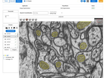
However, with the advancements in computer vision and machine learning, automated semantic segmentation techniques are being employed to enhance semiconductor and wafer inspection. Semantic segmentation refers to the process of classifying and labeling each pixel of an image according to its semantic meaning. By training deep learning models on large datasets of SEM images, manufacturers can achieve accurate and efficient defect detection and classification.
Automated semantic segmentation can significantly improve the speed and accuracy of semiconductor and wafer inspection. It enables manufacturers to quickly identify and classify defects such as cracks, particles, and pattern variations. By automating this process, manufacturers can reduce the inspection time, increase productivity, and minimize the risk of human errors.
Furthermore, the data obtained from automated semantic segmentation can be used for process optimization and yield improvement. By analyzing the defect patterns and distributions, manufacturers can identify the underlying causes, make adjustments to the manufacturing processes, and ultimately improve the overall quality and reliability of the semiconductor devices.
In conclusion, automated semantic segmentation techniques are revolutionizing semiconductor and wafer inspection. They offer a faster, more accurate, and more efficient way of detecting and classifying defects, leading to improved quality control and enhanced manufacturing processes.


