Semiconductor Defect Detection with Bright Field Microscopy and Dark Field Microscopy

Discover how bright field and dark field microscopy are used for semiconductor defect detection, ensuring higher quality and efficiency in manufacturing.
Understanding Bright Field Microscopy: Principles and Applications
Bright field microscopy is one of the most commonly used techniques in semiconductor manufacturing. It operates by transmitting light through a sample, which is then magnified to reveal its structure. The technique is particularly effective for examining transparent or semi-transparent materials, making it ideal for inspecting semiconductor wafers.
In semiconductor fabrication, bright field microscopy is used to detect surface defects such as scratches, contamination, and pattern misalignment. Its simplicity and effectiveness make it a go-to method for routine inspections and quality control processes.
Exploring Dark Field Microscopy: How It Enhances Defect Detection
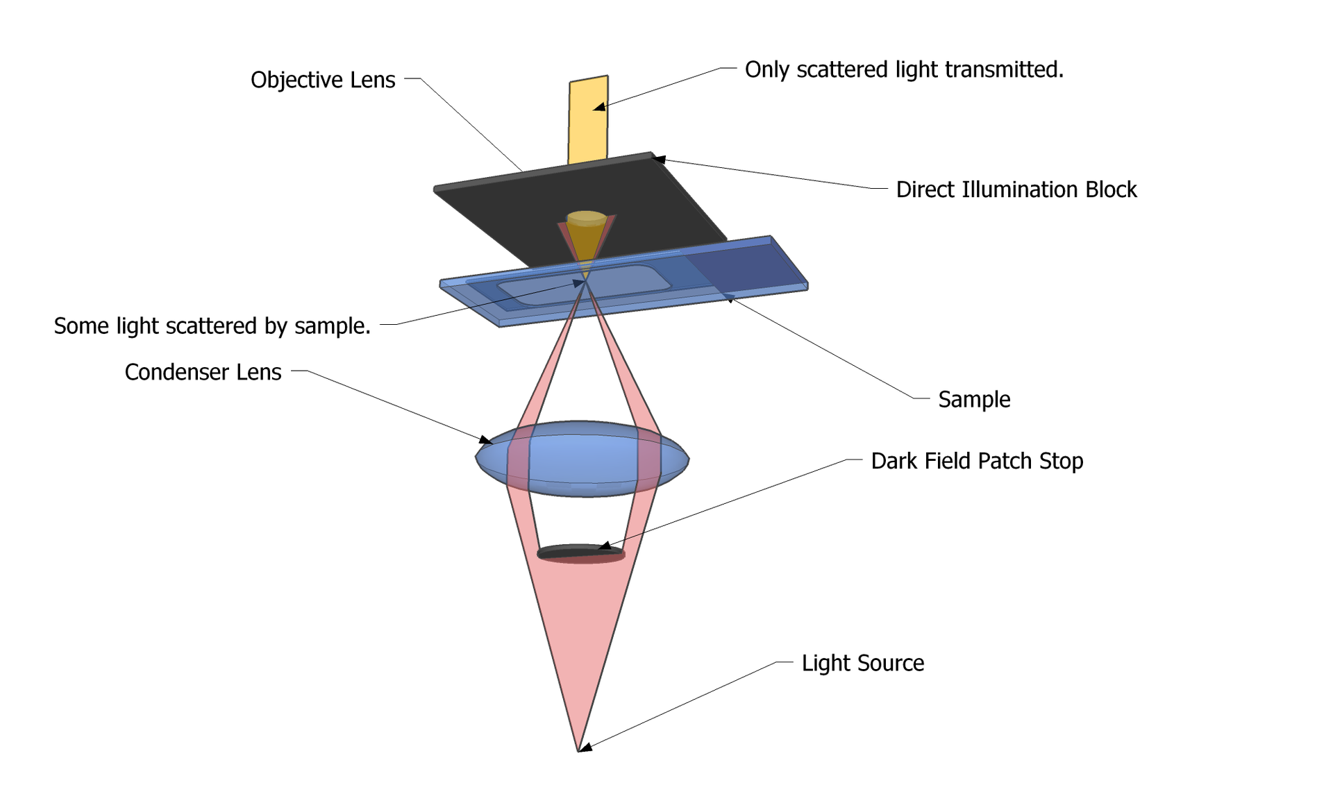
Dark field microscopy takes a different approach by illuminating the sample with light that does not directly enter the objective lens. Instead, only scattered light is captured, which highlights edges and fine details that might be invisible under bright field conditions.
This technique is especially useful for detecting small particles, cracks, and other minute defects on semiconductor surfaces. Dark field microscopy provides higher contrast images, making it easier to identify and analyze defects that could affect the performance of semiconductor devices.
Wafer Inspection
Defects in wafer inspection can generally be categorized into Systematic Defects and Random Defects:
-
Systematic Defects:
Systematic defects occur in the same location and form across multiple dies on a wafer. These defects are often caused by issues in photolithography processes, such as problems with the mask or pellicle. If there is a defect in the mask, it will be replicated onto every die, as the mask's pattern is imprinted onto the wafer during the lithography process.
To inspect for systematic defects, tools such as Dark Field, Bright Field, or E-Beam systems are employed. The inspection process typically involves the following approach:- A defect-free reference die is used as a baseline.
- The tool compares each die against the the reference die(Golden Die).
- Areas that match the Golden Die are marked as "0" (no defect), while discrepancies are marked as "1" (defect detected).
This method allows for the identification of systematic defects across the wafer.
-
Random Defects:
Unlike systematic defects, random defects occur unpredictably at various locations on the wafer. These defects are often caused by particles (e.g., dust, contamination) or other sporadic issues during processing. The same inspection methods used for systematic defects (e.g., Dark Field, Bright Field, E-Beam tools) can also be applied to detect random defects.
Random Defect Inspection with Bright Field
- Bright Field Inspection involves illuminating the wafer surface with light and detecting defects based on the reflected light intensity and characteristics.
- It is effective for detecting random defects, such as:
- Particles
- Scratches
- Contamination
- Surface irregularities
- The technique works well for random defect detection because it provides high sensitivity to small, isolated features and surface changes across the wafer.
- Use Cases:
- Inspecting unpatterned wafers during early stages of manufacturing.
- Detecting particles and scratches introduced during deposition, CMP, or other processes.
Systematic Defect Inspection with Dark Field
- Dark Field Inspection focuses on detecting scattered light, which makes it particularly effective for identifying systematic defects that follow repetitive patterns across the wafer.
- Systematic defects often arise from issues in the photolithography process, such as:
- Mask or pellicle defects
- Misalignments
- Repeating pattern irregularities across dies
- The Dark Field technique enhances sensitivity to subtle differences in scattering caused by repeated pattern anomalies while ignoring regions without scattering.
- Use Cases:
- Inspecting patterned wafers for systematic defects caused by photolithography errors.
- Detecting pattern-related variations across multiple dies.


