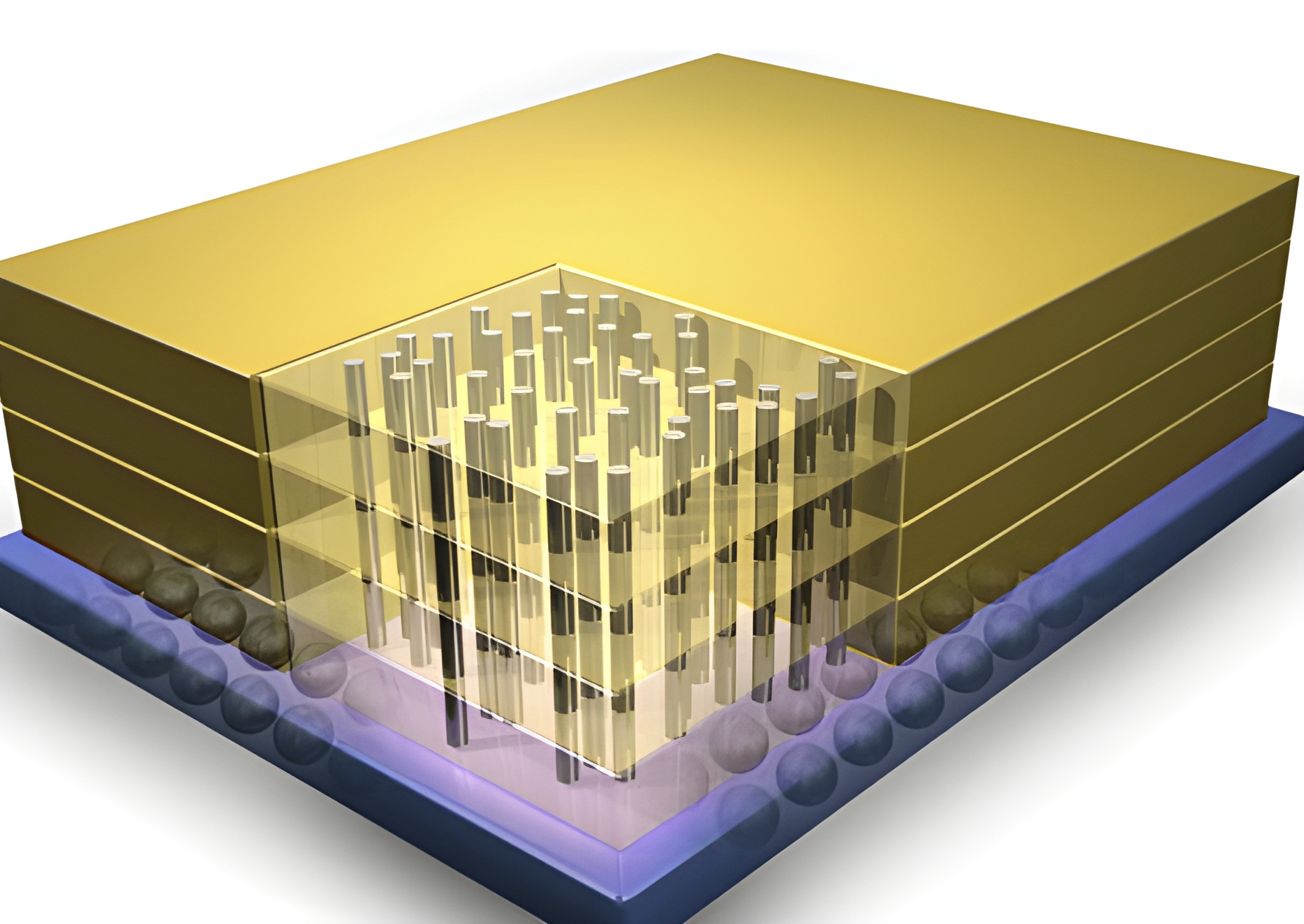
The Power of Through Silicon Via Technology for HBM

Discover the numerous benefits and advantages of through silicon via technology in this informative blog post.
Understanding Through Silicon Via Technology
Through Silicon Via (TSV) technology involves creating vertical electrical connections that pass through the silicon substrate of a chip. These vias enable the integration of multiple layers within a single chip, allowing for increased functionality and improved performance.
TSV technology has revolutionized the semiconductor industry by providing a more efficient and reliable method for interconnecting components on a microscale. By understanding the principles and capabilities of TSV technology, we can fully appreciate its advantages and potential applications.
Enhanced Performance and Speed
One of the key advantages of TSV technology is its ability to enhance the performance and speed of electronic devices. By enabling shorter interconnect lengths and reducing signal propagation delays, TSVs minimize the time it takes for data to travel between different components within a chip.
This improved performance translates into faster data transfer rates, reduced latency, and enhanced overall system efficiency. TSV technology is particularly beneficial in high-speed applications such as data centers, telecommunications, and consumer electronics.
Miniaturization and Integration
TSV technology plays a key role in the miniaturization and integration of electronic devices. By enabling vertical connections, TSVs allow for the stacking of multiple chips or layers within a single package. This vertical integration significantly reduces the footprint of electronic systems, making them more compact and lightweight.
The miniaturization made possible by TSV technology has numerous benefits, including increased portability, improved form factor, and enhanced design flexibility. It enables the development of smaller and more powerful devices, paving the way for advancements in areas such as wearable technology, Internet of Things (IoT), and medical devices.
Microscopy and TSV
Microscopy plays a crucial role in the development and characterization of TSV technology. Various microscopy techniques, such as scanning electron microscopy (SEM) and transmission electron microscopy (TEM), are employed to visualize and analyze the structure and quality of TSVs.
Microscopic inspection allows researchers and engineers to assess the dimensions, alignment, and integrity of TSVs, ensuring their proper functioning and reliability. Microscopy also aids in identifying any potential defects or manufacturing issues that may affect the performance of TSV-based devices.
TEM imaging plays a vital role in the research and analysis of the manufacturing process and potential failures in HBM systems. Utilizing TEM for destructive analysis helps determine the proper penetration of TSVs through the silicon substrate. For example, contemporary HBM memories may encompass thousands of TSVs, with a stitched TEM image serving as a valuable window for conducting failure analysis and optimizing the manufacturing process.
Exploring the Potential of Through Silicon Via Technology in HBM Systems
High Bandwidth Memory (HBM) systems have gained significant attention in recent years for their ability to deliver exceptional memory performance in a compact form factor. TSV technology plays a crucial role in enabling the vertical stacking of memory dies in HBM systems.
By utilizing TSVs, HBM systems achieve high-speed data transfer rates, low power consumption, and increased memory capacity. This makes them ideal for applications that require large amounts of data processing, such as artificial intelligence, graphics-intensive tasks, and high-performance computing.


