Advancements in Wafer Materials: Silicon, SiC, GaAs, GaN

Explore the latest advancements in semiconductor wafer materials, from silicon to GaN, and their impact on the industry.
Types of Wafer Materials
Wafers are made from various types of materials, each with its own unique properties and characteristics.
One common type of wafer material is silicon, which is widely used in the semiconductor industry.
Other types of wafer materials include gallium arsenide, silicon carbide, and gallium nitride.
The choice of wafer material depends on the specific requirements of the application and the desired performance characteristics.
Properties of Silicon Wafers
Silicon wafers are the most commonly used wafer material in the semiconductor industry.
They have excellent thermal conductivity, high melting point, and good electrical properties.
Silicon wafers are also relatively abundant and less expensive compared to other materials.
The properties of silicon wafers can be further enhanced through various manufacturing processes and treatments.
Pros:
-
Abundance: Silicon is one of the most abundant elements on Earth, making silicon wafers readily available and cost-effective compared to other semiconductor materials.
-
High Purity: Silicon wafers can be manufactured with extremely high purity levels, which is crucial for the performance and reliability of integrated circuits.
-
Excellent Semiconductor Properties: Silicon has desirable semiconductor properties, such as a moderate bandgap, good thermal conductivity, and high melting point, making it suitable for a wide range of electronic applications.
-
Versatility: Silicon wafers can be tailored for different applications by adjusting doping levels, surface properties, and crystal orientation.
-
Compatibility: Silicon wafers are compatible with mature semiconductor fabrication processes, allowing for high yields and cost-effective production of integrated circuits.
-
Reliability: Silicon wafers have been extensively studied and characterized over several decades, leading to well-established manufacturing processes and reliable performance.
Cons:
-
Brittleness: Silicon wafers are brittle and prone to breakage, especially during handling and processing. This can lead to yield losses and increased manufacturing costs.
-
Thermal Expansion: Silicon wafers have a relatively high coefficient of thermal expansion, which can cause stress and warpage during high-temperature processes, affecting device performance.
-
Surface Sensitivity: The surface of silicon wafers is sensitive to contamination and defects, which can degrade device performance. Special handling and cleaning procedures are required to maintain surface quality.
-
Power Limitations: Silicon has limitations in high-power and high-frequency applications due to its inherent material properties. Other materials like Silicon Carbide (SiC) and Gallium Nitride (GaN) offer better performance in these areas.
-
Cost of Scaling: While silicon wafer production is cost-effective at large scales, scaling down to smaller feature sizes (nanotechnology) increases manufacturing complexity and costs.
-
Optoelectronic Limitations: Silicon is not an ideal material for optoelectronic devices operating in the visible spectrum due to its indirect bandgap nature. Other materials like Gallium Arsenide (GaAs) and Indium Phosphide (InP) are preferred for these applications.
Exploring the Potential of Silicon Carbide (SiC) Wafers
Silicon carbide (SiC) wafers are gaining popularity in the semiconductor industry due to their unique properties.
SiC wafers have high thermal conductivity, excellent mechanical strength, and can operate at high temperatures.
They are used in applications that require high power and high-frequency operation, such as power electronics and RF devices.
SiC wafers offer improved efficiency and performance compared to traditional silicon wafers.
Pros:
-
High-Temperature Capability: SiC wafers can withstand much higher temperatures than silicon wafers, making them suitable for high-temperature applications such as power electronics and automotive components.
-
High Thermal Conductivity: SiC has excellent thermal conductivity compared to silicon, allowing for efficient heat dissipation in high-power electronic devices, which reduces thermal stress and improves reliability.
-
High Power Density: SiC devices can handle higher power densities than silicon devices, making them suitable for applications requiring high power output in a compact form factor.
-
High Voltage Operation: SiC devices exhibit superior breakdown voltage characteristics compared to silicon, enabling them to operate at higher voltages without breakdown or failure.
-
High-Frequency Operation: SiC devices can operate at higher frequencies than silicon devices, making them suitable for high-frequency switching applications such as RF amplifiers and power converters.
-
Chemical Stability: SiC is chemically inert and resistant to corrosion, making SiC wafers suitable for harsh environments and applications requiring chemical stability.
-
Optoelectronic Properties: SiC exhibits unique optoelectronic properties, including a wide bandgap and high thermal conductivity, making it suitable for optoelectronic devices such as UV photodetectors and LEDs.
Cons:
-
Cost: SiC wafers are typically more expensive than silicon wafers due to the more complex manufacturing process and lower economies of scale. However, the cost has been decreasing with advancements in production technology.
-
Crystal Quality: Achieving high-quality crystalline SiC wafers with low defect densities is challenging, leading to lower yields and higher manufacturing costs compared to silicon wafers.
-
Processing Challenges: SiC wafers are harder and more chemically resistant than silicon wafers, posing challenges for processing techniques such as cutting, polishing, and etching.
-
Heteroepitaxy Challenges: Growth of high-quality SiC epitaxial layers on SiC substrates (homogeneous epitaxy) or on foreign substrates (heteroepitaxy) can be challenging, leading to defects and performance limitations in some devices.
-
Availability of Large Wafers: Large-diameter SiC wafers are not as readily available as silicon wafers, limiting scalability and increasing costs for large-scale production of SiC-based devices.
-
Material Uniformity: Achieving uniform material properties across large SiC wafers is more difficult than with silicon wafers, leading to variations in device performance and reliability.
Exploring the Potential of Gallium Arsenide (GaAs) Wafers
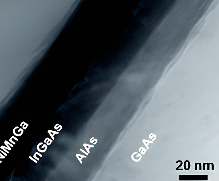
Gallium arsenide (GaAs) wafers are another important material in the semiconductor industry.
GaAs wafers have high electron mobility, allowing them to operate at high frequencies.
They are commonly used in the production of high-speed electronic devices, such as mobile phones and satellite communication systems.
GaAs wafers also exhibit low noise characteristics and are suitable for low-power applications.
Pros:
-
High Electron Mobility: GaAs has higher electron mobility compared to silicon, allowing for faster electron transport and higher device switching speeds. This makes GaAs wafers suitable for high-frequency and high-speed electronic devices such as RF amplifiers and microwave transistors.
-
Direct Bandgap: GaAs has a direct bandgap, unlike silicon which has an indirect bandgap. This property allows GaAs-based devices to efficiently emit and detect light, making them suitable for optoelectronic applications such as LEDs, laser diodes, and photodetectors.
-
Low Noise Characteristics: GaAs-based devices exhibit lower noise levels compared to silicon devices, making them ideal for applications requiring high sensitivity and low noise, such as communication systems and radar.
-
High Breakdown Voltage: GaAs devices can withstand higher breakdown voltages compared to silicon devices, enabling them to operate at higher voltages without failure. This property is advantageous in power electronics and high-voltage applications.
-
High Radiation Resistance: GaAs devices are less susceptible to radiation-induced damage compared to silicon devices, making them suitable for use in space and other high-radiation environments.
-
Compatibility with Compound Semiconductor Materials: GaAs can be alloyed with other compound semiconductor materials such as Aluminum Gallium Arsenide (AlGaAs) and Indium Gallium Arsenide (InGaAs) to tailor its properties for specific applications, allowing for versatile device design and integration.
Cons:
-
Cost: GaAs wafers are generally more expensive than silicon wafers due to the more complex manufacturing process and lower economies of scale. However, the cost has been decreasing with advancements in production technology.
-
Fragility: GaAs wafers are more brittle and fragile than silicon wafers, making them more prone to breakage during handling and processing. This can lead to yield losses and increased manufacturing costs.
-
Thermal Conductivity: GaAs has lower thermal conductivity compared to silicon, which may lead to thermal management challenges in high-power electronic devices. However, this can be mitigated by using heat sinking techniques and thermal interface materials.
-
Material Uniformity: Achieving uniform material properties across large GaAs wafers is more challenging than with silicon wafers, leading to variations in device performance and reliability.
-
Integration Challenges: GaAs-based devices typically require specialized processing techniques and equipment, which may limit their integration with mainstream silicon-based semiconductor manufacturing processes.
-
Susceptibility to Surface Oxidation: GaAs wafers are susceptible to surface oxidation, which can degrade device performance and reliability if not properly controlled through passivation techniques and encapsulation.
Exploring the Benefits of Gallium Nitride (GaN) Wafers
Gallium nitride (GaN) wafers have gained significant attention in recent years.
GaN wafers have excellent electrical and thermal properties, making them suitable for high-power and high-frequency applications.
They are commonly used in the production of power devices, LEDs, and RF devices.
GaN wafers offer higher efficiency and power density compared to other materials.
Pros:
-
Wide Bandgap: GaN has a wider bandgap than silicon, which allows for the fabrication of devices capable of operating at higher voltages, temperatures, and frequencies. This property enables the development of high-performance electronic and optoelectronic devices with improved efficiency and reliability.
-
High Electron Mobility: GaN exhibits high electron mobility, allowing for faster electron transport and higher device switching speeds compared to silicon. This property is beneficial for applications requiring high-frequency operation, such as RF amplifiers and power converters.
-
High Power Density: GaN-based devices can handle higher power densities than silicon devices, making them suitable for high-power electronic applications such as power amplifiers, DC-DC converters, and power supplies.
-
High Thermal Conductivity: GaN has high thermal conductivity, allowing for efficient heat dissipation in high-power electronic devices. This property helps reduce thermal stress and improves device reliability, especially in applications with high power dissipation.
-
Chemical Stability: GaN is chemically stable and resistant to oxidation, making GaN wafers suitable for use in harsh environments and applications requiring chemical stability.
-
Optoelectronic Properties: GaN-based materials exhibit excellent optoelectronic properties, including high luminescence efficiency and emission in the blue to ultraviolet spectrum. This makes GaN wafers ideal for applications such as blue LEDs, laser diodes, and high-efficiency lighting.
Cons:
-
Cost: GaN wafers are typically more expensive than silicon wafers due to the more complex manufacturing process and lower economies of scale. However, the cost has been decreasing with advancements in production technology.
-
Crystal Quality: Achieving high-quality crystalline GaN wafers with low defect densities is challenging, leading to lower yields and higher manufacturing costs compared to silicon wafers.
-
Heteroepitaxy Challenges: Growth of high-quality GaN epitaxial layers on foreign substrates (heteroepitaxy) can be challenging, leading to defects and performance limitations in some devices.
-
Material Uniformity: Achieving uniform material properties across large GaN wafers is more difficult than with silicon wafers, leading to variations in device performance and reliability.
-
Integration Challenges: GaN-based devices typically require specialized processing techniques and equipment, which may limit their integration with mainstream silicon-based semiconductor manufacturing processes.
-
Susceptibility to Trap States: GaN-based devices are susceptible to trap states and surface/interface defects, which can degrade device performance and reliability if not properly controlled through passivation techniques and defect engineering.


