Harness the Power of Computer Vision to Streamline Failure Analysis
Discover the power of uncovering minuscule imperfections in the nano world, all at lightning speed.
Even the tiniest flaws in the micro world can unleash significant complications in the larger realm of technology.
As nanotechnology, material science, and semiconductor manufacturing technologies continue to evolve, everything gets smaller. However, the nanotechnology also amplifies the impact of minor defects on semiconductors, materials, and MEMS.
Fortunately, Deep Block's cutting-edge machine vision technology, integrated with its ultra-high-resolution microscope image analysis, emerges as the ultimate solution to conquer these intricate challenges and eliminate imperfections.
Discover the countless challenges posed by large-volume, high-resolution images.
Discover the incredible challenges presented by large-volume, high-resolution images. These images are truly massive in terms of their size. Simply rendering high-resolution images on the front-end is a complex task, and combining such enormous images with machine vision technology poses an even greater challenge.
Due to their size and resolution, these images need to be divided and analyzed. However, this process brings a lot of problems, including speed problem and the potential loss of features when analyzing the countless pieces of the image.
Fortunately, by harnessing the power of Deep Block's computer vision technology specifically designed for ultra-high resolution images, your microscopic image analysis can be effortlessly automated, making it incredibly easy.
Failure Analysis & Characterization
While the thin film remains unseen to our unaided vision, it reveals itself as a THICK layer when magnified by an electron microscope.
We are very interested in the step coverage, morphology, and composition of each layer, but we rely on our eyes to see the thickness and connectivity of the numerous gates and metals that exist in the HUGE WAFER OCEAN.
Take control of your Micrograph analysis today without any coding knowledge. Create your own machine learning model and harness the power of our state-of-the-art machine vision technology. Trust Deep Block to gain insight into thin film morphology.
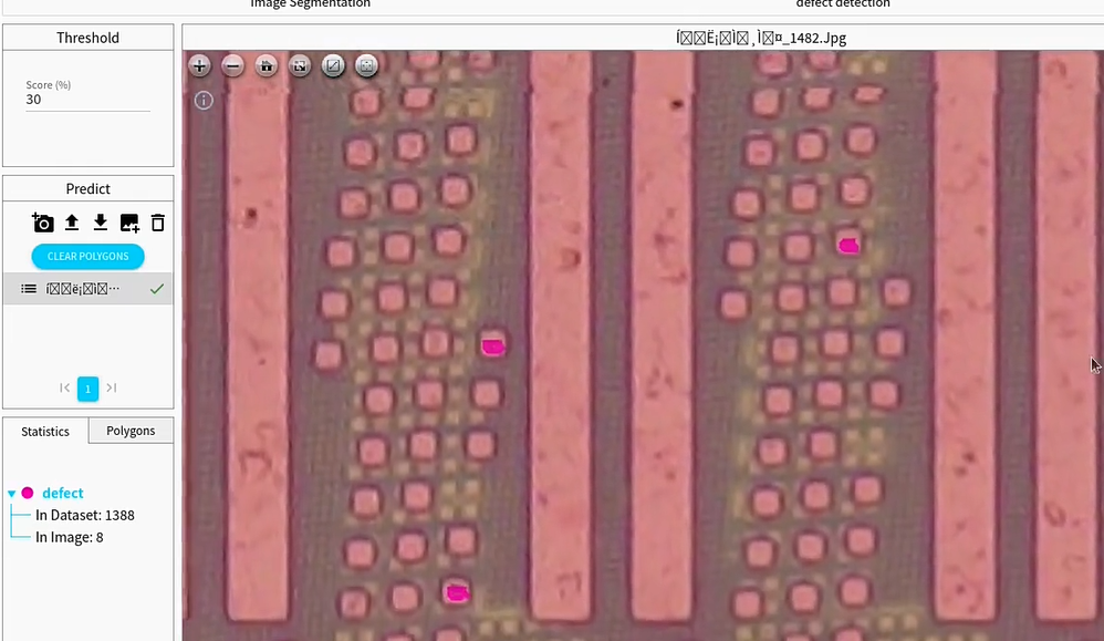
Large Area Analysis
Under a microscope, the area of a single wafer or chip is too vast.
Use multi-beam SEM to capture the large area, or prepare stitched micrographs, and then upload the image into DEEP BLOCK.
For unrivaled efficiency in LARGE AREA ANALYSIS, DEEP BLOCK stands as your premier choice.
For those seeking an integrated solution, we extend on-premise hardware and software to streamline your analysis within your own facility.
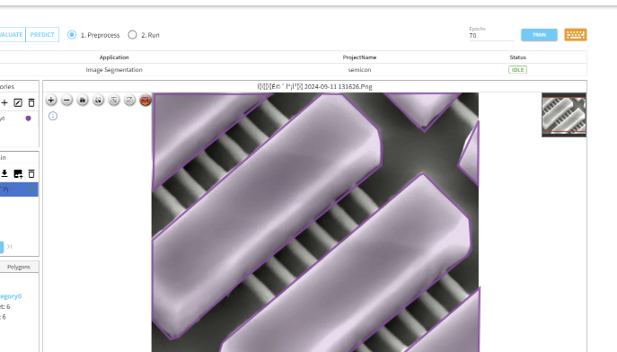
Process Engineering
Guarantee the accuracy of each layer's deposition and review your production procedure.
Minor deviations in layer thickness or unexpected errors in the etching process can significantly compromise the integrity of the chip manufacturing operation, leading to product failure.
The introduction of advanced technologies, such as glass substrates and hybrid bonding, necessitates the adoption of microscopy for their inspection.
Leverage the transformative potential of machine learning to seamlessly assess layer thickness and structure, substantially improving your quality assurance protocols.
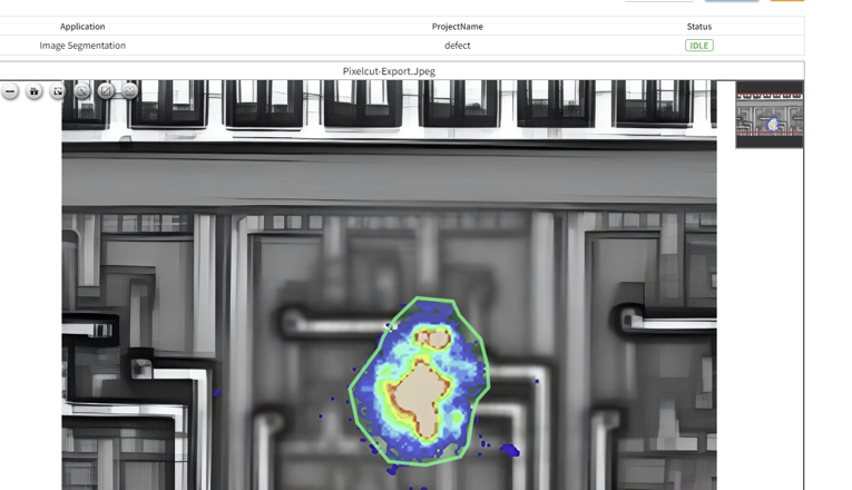
Emission Microscopy
For failure analysis at the PCB and packaging level, the Emission Microscope is effectively utilized.
Analyzing failures in boards and circuits is essential for MEMS production and modern IC packaging technologies.
Use the Emission Microscope to monitor the thermal radiation across the entire circuit, and with Deep Block, quickly pinpoint the cause and location of failures.
Stitched TEM, SEM
The tiny chip is TOO LARGE under the microscope.
Whether you want to cut the chip and look at its cross section, or inspect the entire surface, DEEP BLOCK's LARGE-scale image analysis technology will be of great help!
The demand for Electron Microscopy is significantly boosted by the NXE systems, packaging technologies, and High Bandwidth Memory (HBM).
As vias and layers shrink in size, the details we need to observe become increasingly minuscule.
We are tasked with the intricate challenge of discerning the smallest of structures, interpreting very thin films as mere lines, dots, or substantial layers.
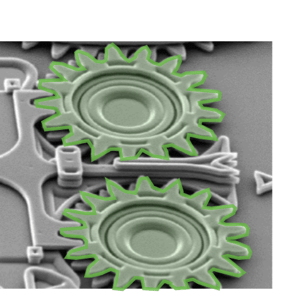
MEMS
Characterizing MEMS structures is crucial for crafting accurate sensors and averting malfunctions.
Precisely segmenting and automating the analysis of your MEMS structures is key to achieving this.
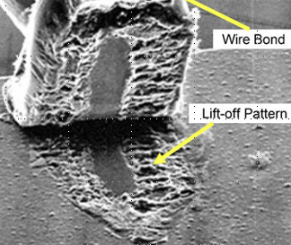
Packaging
Microscopes play a pivotal role in every aspect of packaging processes, encompassing techniques such as through-glass via and hybrid bonding. Tackle your failure analysis with Deep Block!
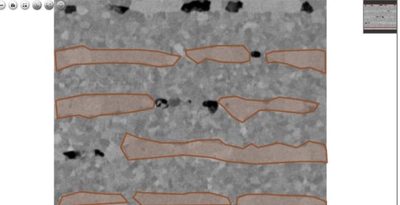
Multilayer Ceramic Capacitor(MLCC)
An MLCC is composed of over 600 layers of Ni electrodes and fine barium titanate powder. When an MLCC is captured using an SEM or optical microscope, its cross-section appears very tall and extremely long horizontally. Utilize Deep Block for failure analysis, thin film evaluation, and capacitance evaluation to create smaller, cheaper, high-performance capacitors.
The world's fastest imagery analysis solution.

10 GP pixels
Max file resolution
or 100,000 x 100,000 pixels images.

40 GB
Max file size
vs. 1 GB with our competitors.

10GB/sec.
Processing
speed.

0.9 AP
Highly accurate prediction
when detecting objects.

0.9 Recall
Highly reliable detection
with minimum false negatives.
When confidentiality and security are not only buzzwords.
At Deep Block, we understand the needs of large enterprises and public organizations and are willing to work closely with your team to ensure a smooth deployment and usage of the solution.
Advanced Security
Get additional security features to fit your compliance needs like VPN connection, monitoring, fixed IP, and others.
Custom Domain
Get your own enterprise account, allocated users seats, and branded domain.
Self-Hosting Support
Host Deep Block in your own private cloud or on-premise for maximum security.
Access Provisioning
Define user accesses and privileges to make sure that the right person has access to the right information.
Workflow Customization
Request custom interfaces, features, or workflows directly from our engineering team.
Premium Support
Our support team will be monitoring your needs on the clock to ensure a smooth Deep Block experience.
Interested? Let's get in touch!
Whether it is to get a demo of our Deep Block Platform, inquire about our learning courses, join our latest Bootcamp or explore custom solutions with us, we will be happy to help!

