Mastering Epitaxial Growth Techniques

Understand epitaxial growth techniques with this comprehensive guide.
Utilizing the Czochralski method, epitaxial growth serves as a fundamental process essential for creating crystal Silicon.
Understanding Epitaxial Growth
Epitaxial growth refers to the process of growing a thin film or layer of material on a substrate with a crystalline structure that mimics the arrangement of atoms in the substrate. This technique is widely used in the semiconductor industry to produce high-quality films with controlled properties.
During epitaxial growth, the atoms or molecules from the source material are deposited on the substrate in a way that allows them to align with the existing crystal lattice. This alignment is crucial for the film to inherit the structural and electronic properties of the substrate.
Understanding the principles and mechanisms behind epitaxial growth is essential for mastering this technique and achieving desired film properties.
Key Factors Influencing Epitaxial Growth
Several factors can influence the epitaxial growth process and the resulting film quality. These factors include:
1. Substrate choice: The choice of substrate material and its crystal orientation play a crucial role in determining the epitaxial growth behavior. Different substrates have different lattice constants and crystal structures, which can affect the film's nucleation, growth rate, and crystal quality.
2. Epitaxial growth temperature: The temperature at which the deposition takes place can significantly impact the film's morphology, crystal structure, and defect density. It is important to optimize the growth temperature to achieve the desired film properties.
3. Epitaxial growth rate: The rate at which the material is deposited onto the substrate can influence the film's crystal quality and defect density. Controlling the growth rate is essential to achieve uniform and high-quality films.
4. Surface preparation: Proper surface cleaning and preparation are crucial for successful epitaxial growth. Any contaminants or oxide layers on the substrate surface can hinder the growth process and affect the film's quality.
By understanding and controlling these key factors, researchers and engineers can optimize the epitaxial growth process and produce films with desired properties.
Advanced Techniques for Epitaxial Growth
In addition to the fundamental principles of epitaxial growth, there are several advanced techniques that can further enhance the control and quality of the grown films. These techniques include:
1. Molecular Beam Epitaxy (MBE): MBE is a widely used epitaxial growth technique that allows precise control over the deposition process at the atomic level. It involves evaporating the source material in a high vacuum environment, enabling the growth of highly crystalline films with excellent control over layer thickness and composition.
2. Metal-Organic Chemical Vapor Deposition (MOCVD): MOCVD is another commonly used technique for epitaxial growth, especially for compound semiconductors. It involves the reaction of metal-organic precursors in a heated chamber, resulting in the deposition of crystalline films. MOCVD offers high growth rates and scalability, making it suitable for industrial applications.
3. Hybrid Approaches: Some advanced techniques combine different epitaxial growth methods to take advantage of their individual strengths. For example, pulsed laser deposition (PLD) combines the precision of MBE with the scalability of MOCVD, resulting in high-quality films with complex compositions.
By utilizing these advanced techniques, researchers and engineers can push the boundaries of epitaxial growth and develop materials with tailored properties for various applications.
Characterization Methods for Epitaxial Films
To assess the quality and properties of epitaxial films, various characterization methods are employed. These methods include:
1. X-ray Diffraction (XRD): XRD is a widely used technique for determining the crystal structure, lattice parameters, and strain in epitaxial films. By analyzing the diffraction patterns produced by X-rays interacting with the film, valuable information about the film's crystallographic properties can be obtained.
2. Scanning Electron Microscopy (SEM): SEM is used to visualize the surface morphology and topography of epitaxial films. It provides high-resolution images that reveal details about the film's growth mode, defects, and uniformity.
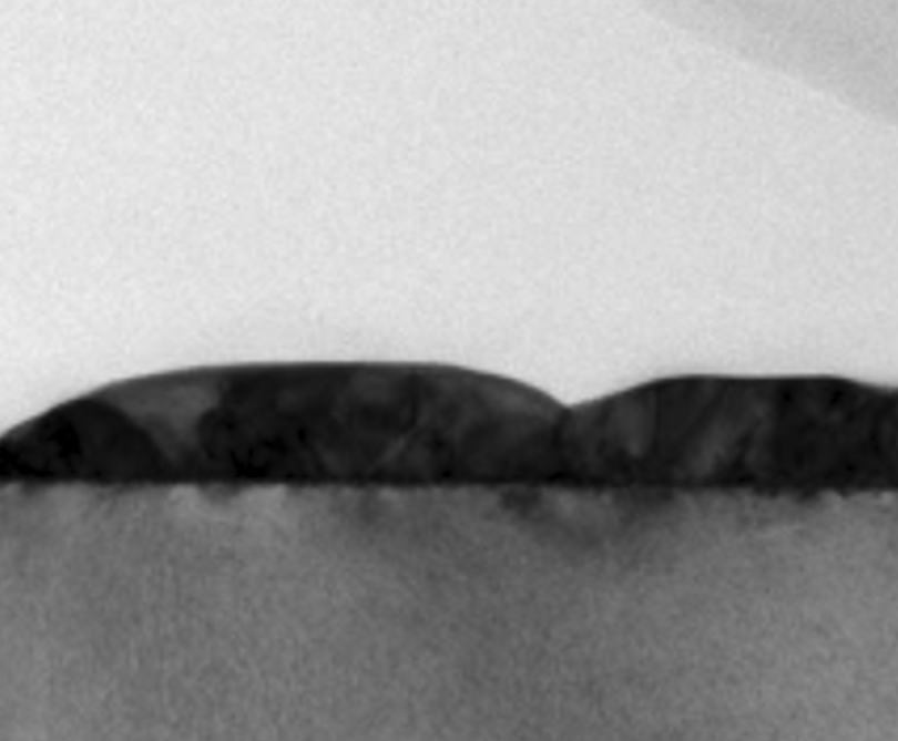
3. Transmission Electron Microscopy (TEM): TEM allows for detailed analysis of the internal structure and defects in epitaxial films at the atomic scale. It provides valuable information about the film's crystal quality, dislocations, and interfaces.
4. Secondary Ion Mass Spectrometry (SIMS): SIMS is a technique used to analyze the elemental composition and depth profiles of epitaxial films. It can provide information about impurity concentrations, dopant distribution, and diffusion profiles.
By employing these characterization methods, researchers can gain insights into the structural, morphological, and compositional properties of epitaxial films, enabling them to optimize the growth process and assess the film's suitability for specific applications.
Assessment of Crystal Quality using Microscopy
Microscopy techniques play a crucial role in assessing the crystal quality of epitaxial films. By examining the film's structure and defects at various length scales, researchers can evaluate its suitability for different applications. Some microscopy techniques commonly used for crystal quality assessment include:
1. Atomic Force Microscopy (AFM): AFM enables the visualization of surface topography and roughness at the nanoscale. It can provide information about the film's growth mode, step edges, and surface defects.
2. Scanning Tunneling Microscopy (STM): STM allows for atomic-scale imaging of the film's surface. It can reveal details about the film's crystal structure, defects, and atomic arrangement.
3. Electron Backscatter Diffraction (EBSD): EBSD is used to analyze the crystallographic orientation and grain boundaries in epitaxial films. It can provide information about the film's texture, strain, and grain size.
By utilizing these microscopy techniques, researchers can gain valuable insights into the crystal quality of epitaxial films and make informed decisions regarding their use in various applications.


